Hi!
Today we introduce you to the idea of the top PCB (http://en.wikipedia.org/wiki/Printed_circuit_board) that we have!
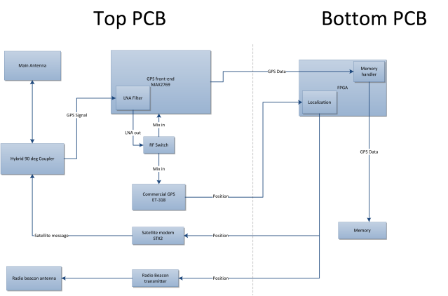
Sorry about the small font, but I’ll try to explain how it works!
The main purpose of the top PCB is to collect GPS data from the main antenna during the fall of the FFUs. The signals from the main antenna first go through the hybrid 90 deg coupler (described by Ólafía a few days ago) and then into a Low Noise Amplifier (or LNA – http://en.wikipedia.org/wiki/Low-noise_amplifier) in the brains of the GPS experiment; the MAX2769 chip. It’s this chip that takes the raw GPS signal, runs it through a couple of filters, sprinkles some magic on it, and then outputs the digital GPS data. It’s this data that we save, and then when the probe is safely on the ground again, we analyse it and get our solution!
The three other main parts of the top PCB is part of the localization system. It’s this system that ensures that we find our poor probes when they lie there all alone in the harsh landscape of Kiruna. Here is a quick description of their job:
Commersial GPS – After parashute deployment, we need to know where we are right away so saving the raw GPS data is no good. We need to calculate a position on the fly, quick and dirty! This chip does it all! Signal in, position out. It’s as easy as that! (almost 😉 )
Satellite modem STX2 – When we have the position we send it to ourselves through the Globalstar satellite telephone system. This chip does just that!
Radio Beacon transmitter – Close to the probe we also constantly send out our position with a radio beacon. This is partly for redundancy in the system above, but also for the helicopter being able to take bearing on the probe and find it when we get close!
That’s all for now! Next time I might have the pleasure to give you some schematics of the board itself!
/Leo

Hello Leo, My name is Fawaz and Im doing my master in GPS receiver design on FPGA,
I saw your great experiment and I noticed you used MAX2769EVKIT, I would like to ask you sir, can you use this kit to get some output ( I Mean digital output) for the FPGA receiver? because Im planning to purchase one.
Thanks
Hello!
All the information about the MAX2769 is available in the data sheet! 🙂
http://www.alldatasheet.com/datasheet-pdf/pdf/348496/MAXIM/MAX2769.html
Does that answer your question?
/Leo
Hello Mr. Leo.
I have this datasheet and I know this pcb can produce (sign,mag). but can we get these outputs from the development kit? I saw there are some jumpers pins named as (I0, I1,Q0..) in this kit, did you try them? did you get any digital output?
Aahh sorry didn’t see that you meant the EV kit.
Well in our experiment we don’t use the FPGA as a receiver (which you are if I understand you correctly). All we do is send the data to the FPGA which then saves it to a memory for post-processing in a MATLAB receiver. The data coming in is sign,mag. The reason that we use this approach and not all 4 channels (I0,I1,Q0,Q1) is simply because it has been proven to work in our setup! Since the EV kit outputs data feeds we needed to save these on a memory to be able to use our receiver. And our experiment Pcbs do not allow for this type of connection with the EV kit. Therefor we had to use a custom made pcb “logger board” that had the capability to take the data from the EV kit and save it for processing.
I did however never personally use the EV kit to get actual data and characterise the performance of the chip with different settings. I think the reasoning was that there was a too big of a difference between the EV kit setup that we had to use and the FFU setup that we had with our custom antenna, hybrid coupler and all. It might be usefull if you fully wanted to investigate different settings in the max2769 but we prioritised other things since we have a tight schedule.
Aha so now I got the idea, but you could use these pins or giving an output right?
you can use my design, I got Namuru GPS, through this design you have to use RF capable of sending a data for you (sign,mag) and use it as input to the FPGA (Baseband), and there is a software running on NIOS II processor inside the FPGA and make a real time GPS system.
Thanks for your reply
Hello Dear I hope you are fine and doing well,
During your Work on MAX2769EVKIT+, did you connect it with (+3,+5,-5) power supply?
or we can use just one of them like (+5 GND).